|
ABSTRACT
In this sub-project, we will explore the designs of
high-speed switches and extend our results on Gigabit Ethernet Service Switch (GESS)
to Gigabit Ethernet Multi-Service Switch (GEMSS).
1. Design and implementation of high-speed
switches that scale with the speed of fiber optics.
One of the main objectives of this sub-project is to design and implement high
speed switches that scale with the speed of fiber optics. Our approach will be
based on the load-balanced Birkhoff-von Neumann switch architecture developed in
the first phase of our PPAEU project.
2. Design and implementation of high-speed multi-service switch.
The second main objective of this
sub-project is to design and implement policy-based high speed multi-service
switch based on network processor hardware platform to provide gigabit level
multi-service, such as VPN, QoS mobility management, Ipv4/Ipv6 translation,
intrusion prevention, content filtering, anti-virus on the fly, etc, over
LAN/MAN environments. Our approach will be based on the network processor-based
service switch platform developed in the first phase of our PPAEU project.
CONTENTS
In this sub-project, we will explore the designs of
high-speed switches and extend our results on Gigabit Ethernet Service Switch (GESS)
to Gigabit Ethernet Multi-Service Switch (GEMSS).
1. Design and implementation of high-speed
switches that scale with the speed of fiber optics.
One of the main objectives of this sub-project is to design and implement high
speed switches that scale with the speed of fiber optics. Our approach will be
based on the load-balanced Birkhoff-von Neumann switch architecture developed in
the first phase of our PPAEU project.
Switch Architecture
Most of the switches in the market (e.g., Ether switches) are based on the
so-called shared memory switch architecture. In such a switch architecture,
packets are stored and forwarded in a common shared memory. As the speed of
fiber optic advances, the memory access speed becomes a bottleneck for the share
memory switch architecture. With the current memory technology, a shared memory
switch is limited to the speed of 50 Gbits/sec. To go beyond such a speed, one
has to use parallel-buffered switch architecture to acquire the needed speedup.
One common approach, known as the input-buffered switch architecture, is to have
parallel buffers in front of a (crossbar) switch fabric. In an input-buffered
switch, time is synchronized and slotted so that packets of the same size can be
transmitted in parallel. As there are multiple buffers (memories), the key
problem of input-buffered switch is to solve the conflict of parallel memory
access.
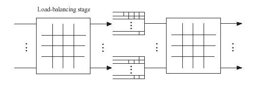

Figure 1.2. The folded version of the mailbox switch.
Switch Fabric
 (1)
(1)
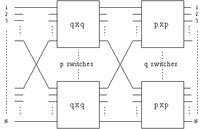
Figure 1.3. A two-stage construction of an NxN symmetric TDM switch
fabric.
Even though
an N×N symmetric TDM switch can be implemented by an N×N crossbar
switch, one of our key innovations show that an N×N symmetric TDM
switch can be recursively constructed with O(Nlog N) complexity. In
Figure 1.3, we show a two-stage construction of an N×N symmetric TDM
switch (with N=pq). The first stage consists of p q×q symmetric TDM
switches (indexed from 1, 2, ..., p) and the second stage consists of
q p×p symmetric TDM switches (indexed from 1, 2, ..., q). These two
stages of switches are connected by the perfect shuffle, i.e., the
lth output of the kth switch at the first stage is
connected to the kth input of the lth switch at the
second stage. Also, index the N inputs and outputs from 1 to N. The
N
inputs of the N×N switch are connected to the inputs of the switches
at the first stage by the perfect shuffle.
Figure 1.4. A 256x256 symmetric TDM switch with 2x2 switches via the
recursive construction.
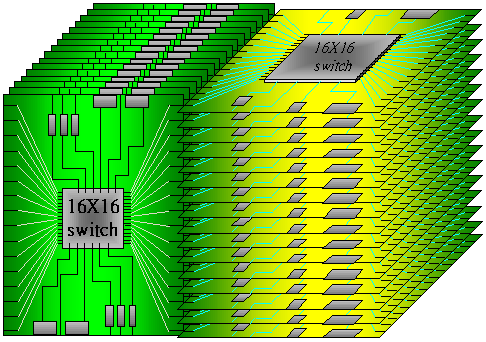
Figure 1.5. A
3D-construction of a 256x256 symmetric TDM switch fabric.
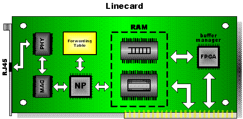
Figure 1.6. The architecture
for a linecard.
2. Design and implementation of high-speed multi-service switch.
The second main objective of this
sub-project is to design and implement policy-based high speed multi-service
switch based on network processor hardware platform to provide gigabit level
multi-service, such as VPN, QoS mobility management, Ipv4/Ipv6 translation,
intrusion prevention, content filtering, anti-virus on the fly, etc, over
LAN/MAN environments. Our approach will be based on the network processor-based
service switch platform developed in the first phase of our PPAEU project.
GESS Switch
Architecture

Figure 1.7.
The chassis based gigabit Ethernet service switch.
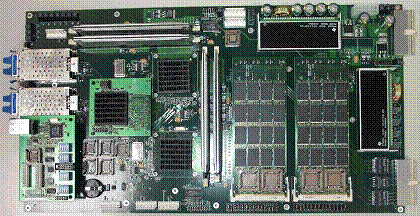
Figure 1.8. The gigabit service module.
GEMSS
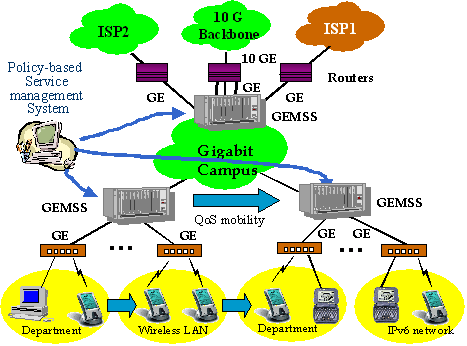
Figure 1.9. The deployment of the GEMSS on the gigabit campus
network.
REFERENCES
[1.1]
T. Anderson, S. Owicki, J. Saxes
and C. Thacker, “High speed switch scheduling for local area networks,”
ACM Trans. on Computer Systems, Vol. 11 , 1993, pp. 319-352.
[1.2]
C. S. Chang, D. S. Lee and Y. S.
Jou, “Load balanced Birkhoff-von Neumann switches, part I: one-stage
buffering,” Computer Communications, Vol. 25, pp. 611-622, 2002
[1.3]
C. S. Chang, D. S. Lee and C. M.
Lien, “Load balanced Birkhoff-von Neumann switch, part II: Multi-stage
buffering,” Computer Communications, Vol. 25, 2002, pp. 623-634
[1.4]
C. S. Chang, D. S. Lee, and C.
Y. Yue, “Providing guaranteed rate services in the load balanced
Birkhoff-von Neumann switches,” Proceedings of IEEE INFOCOM, 2003.
[1.5]
C. S. Chang, D. S. Lee and Y. J.
Shih, “Mailbox switch: a scalable two-stage switch architecture for conflict
resolution of ordered packets,” preprint, 2004.
[1.6]
J. Dai and B. Prabhakar, “The
throughput of data switches with and without speedup,” Proceedings of
IEEE INFOCOM, Tel Aviv, Isreal, March, 2000, pp. 556-564
[1.7]
M. J. Karol, M. G. Hluchyj, and
S. P. Morgan, “Input Versus Output Queueing on a Space-Division Packet
Switch,” IEEE Trans. Commun., Vol. COM35, NO.12, Dec. 1987.
[1.8]
Y. Li, S. Panwar and H. J. Chao,
“On the performance of a dual round-robin switch,” Proceedings of IEEE
INFOCOM, 2001, pp. 1688-1697.
[1.9]
N. McKeown, “Scheduling
algorithms for input-queued cell switches,” PhD Thesis. University of
California at Berkeley, 1995.
[1.10]
N. McKeown, V. Anantharam
and J. Walrand, “Achieving 100% throughput in an input-queued switch,”
Proceedings of IEEE INFOCOM, 1996, pp. 296-302.
[1.11]
A. Mekkittikul and N.
McKeown, “A practical scheduling algorithm to achieve 100% throughput in
input-queued switches,” Proceedings of IEEE INFOCOM, 1998.
[1.12]
N. F. Huang and S. M.
Zhao, “A Novel IP Routing Lookup Scheme and Hardware Architecture for
Multi-Gigabit Switch Routers,” IEEE Journal of Selected Areas on
Communications (IEEE JSAC), Vol. 17, No.6, June 1999, pp.1093-1104.
[1.13]
N. F. Huang and T. Liu, ”
A Novel URL Lookup Engine for Content-Aware Multi-Gigabit Switches,”
submitted for publication.
[1.14]
N. F. Huang and T. Liu, ”
A Fast String Matching Algorithm for Network Processor based Intrusion
Detection System,” submitted for publication.
Copyright Computer and Communication Research Center - All Rights
Reserved
|